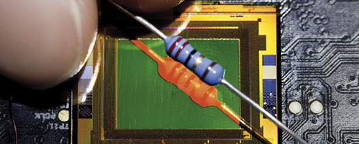
Our long-term experience in design of analog, mixed-signal, digital IC provides a basis for the realization of customized solutions. The typical applications follow the slogan more-than-moore, in the integration of additional functions. Therefore the standard CMOS processes is disrupted namely the post-treatment is implemented (deposition of organic emitting or photo diodes). Fraunhofer FEP is fabless and works with various CMOS-foundries. For the post-treatment Fraunhofer FEP can use 200 mm cleanroom.
IC and system design
Our offer
Design of analog, digital and mixed-signal IC based on the state of the art. Typical CMOS-processes: : 0.13 μm / 0.18 μm / 0.35 μm
Design steps:
- Concept
- Modelling
- System design
- Circuit design
- Simulation
- Layout
- Verification
- Coordination of external CMOS-wafer fabrication as a contractor between the customer and the foundry
- Test
- Commissioning
- Life-time tests
Applications
- Unidirectional OLED microdisplays (OLED-on-silicon)
- Bidirectional microdisplays with embedded image sensors
- Hall sensor
- Display controller for passive OLED
- Displays
- Radiation detector
- Sensor signal processing
Equipment
- Post-processing of Si-wafers
- OLED/OPD deposition
- Encapsulation
- Development of optical filters
- Structuring with shadow masks or photolithography
- Wafer integration
 Fraunhofer Institute for Organic Electronics, Electron Beam and Plasma Technology FEP