 Fraunhofer Institute for Electron Beam
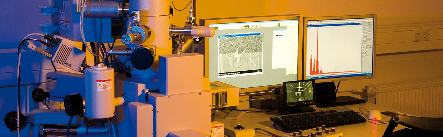
The department materials analysis at Fraunhofer FEP has versatile methods for characterization of thin films and surfaces. The equipment and the wide analytical experience of our staff are available for the product and technology development of our institute and are offered as a service to our customers. Typical applications areas are layers for optics, sensor technology, displays, photovoltaic, packaging, corrosion and wear resistance.
Materials analysis
Structure and microstructure
- FE scanning electron microscope (FE-REM), SU8000 (Hitachi)
- Ion preparation technique for cross sections, Cross Section Polisher SM-09010 (JEOL)
- Metallographic preparation technique (Strues) and optical microscope Polyvar 2 Met (Reichert)
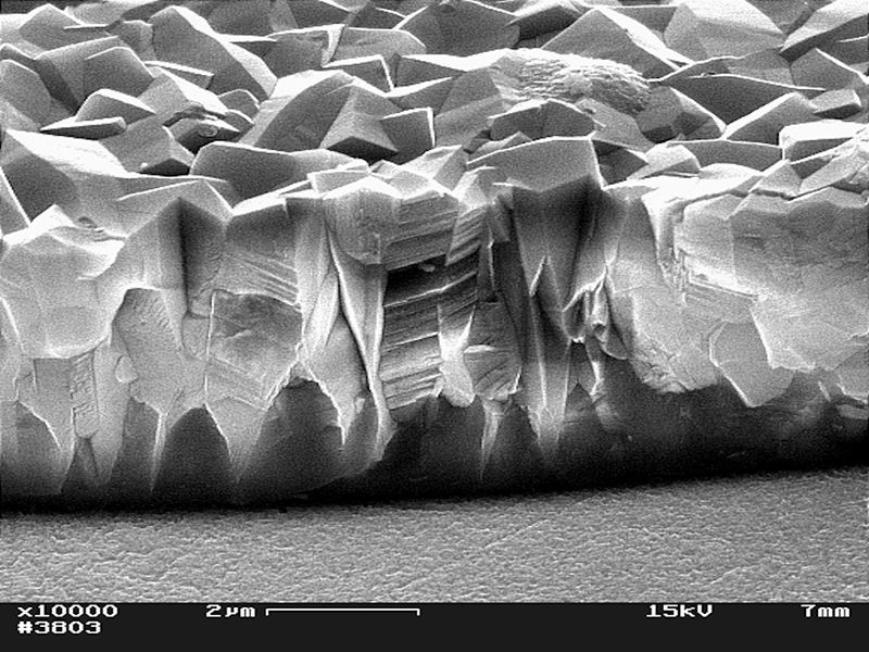
Cross fracture and surface of an Al2O3 wear resistant layer
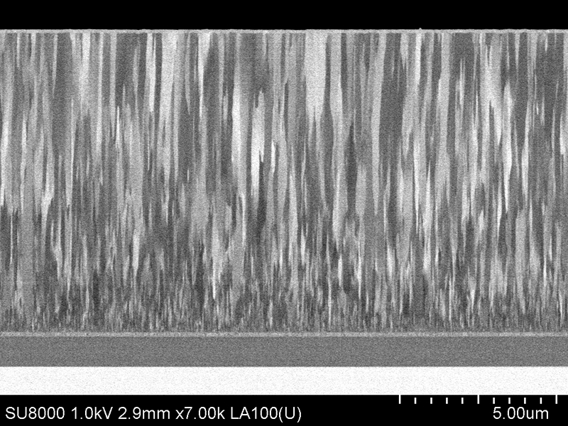
Microstructure of an AlN layer for piezoelectric applications
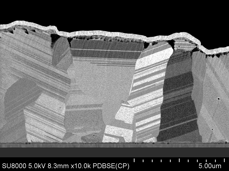
Ion polished cross section of a CdTe solar cell
Chemical composition
- Energy-dispersive X-ray spectroscopy (EDS), Apollo XV (EDAX)
- Glow discharge optical emission spectroscopy (GD-OES), GD-Profiler 2 (HORIBA Jobin Yvon)
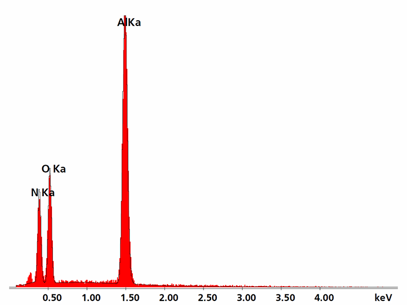
EDS spectrum of an AlOxNy layer
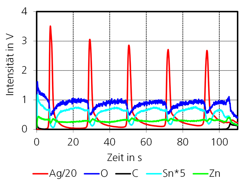
GD-OES Intensity time profile of a solar control layer system with 5 × 10 nm silver layers
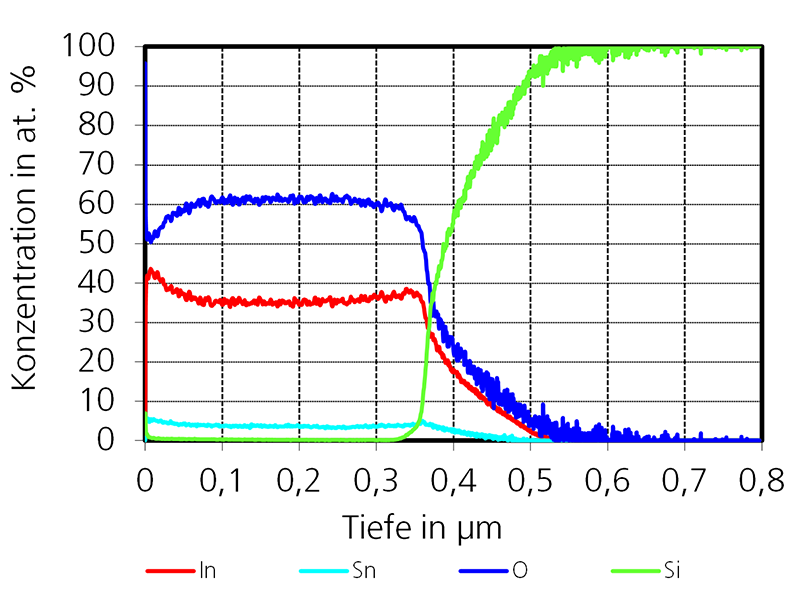
GD-OES Chemical depth profile of a transparent and conductive ITO layer
Topography, surface and layer thickness
- Atomic force microscopy (AFM), Explorer (Topometrix)
- Surface profilometry, P15-LS (Tencor)
- Calotest (CSEM)
- Contact angle, OCA 20 (Data Physics)
Surface of a FTO layer
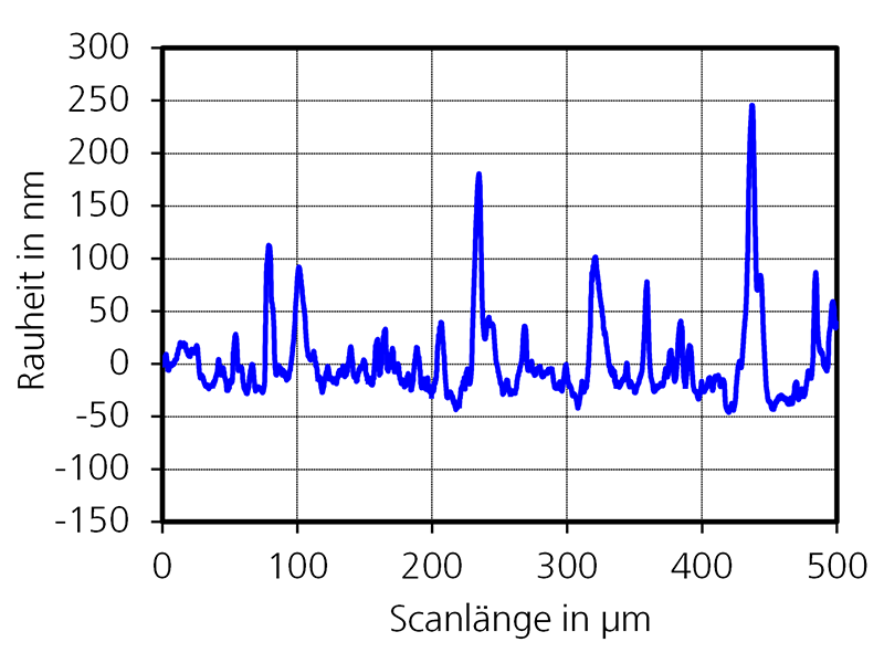
Roughness scan of a PET film
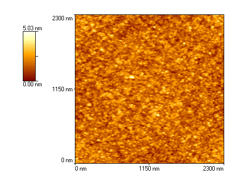
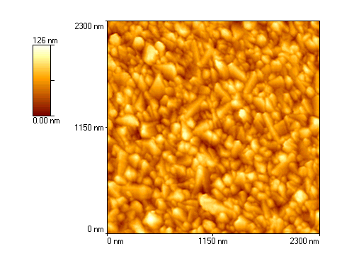
Surface of a very smooth SiO2 layer
Permeation barrier
- Water vapor permeability (WVTR) according to DIN EN ISO 15106-03, WDDG (Brugger Feinmechanik);
Measurement range 10-3 to 10 g/(m2d) - Water vapor permeability, HiBarSens (Sempa);
Measurement range 10-6 to 10-3 g/(m2d) - Oxygen permeability (OTR) according to DIN 53380-3 and ASTM D 3985-05, OX-TRAN 2/20 (Mocon);
Measurement range 0.1 to 200 cm3/(m2d bar)
Optical, mechanical and electrical properties
- Spectroscopic ellipsometry SE850 (SENTECH)
- UV/VIS/NIR spectroscopy, Lambda 950 (Perkin Elmer)
- Haze measurement, Haze-guard plus (BYK-Gardner)
- Hardness and Young’s modulus, Nano Indenter XP (MTS)
- Film stress, Profilometer P15-LS (TENCOR)
- Scratch adhesion test, MST4 (CSEM)
- Abrasion resistance (Taber Abraser)
- I-U curve of solar cells (Sun 300, LOT)
- Quantum efficiency, Oriel IQE-200 (Newport)
- Photo and dark conductivity (SÜSS Prober and Keithley)
- Electrical four point probe, FPP 5000 (Veeco)
Determination of optical properties by spectroscopy ellipsometry (SE850; Sentech)
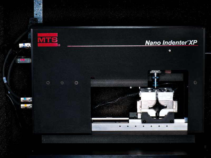
Determination of hardness and Youngs modulus of thin layers by Nanoindentation (Nano Indenter XP; MTS)
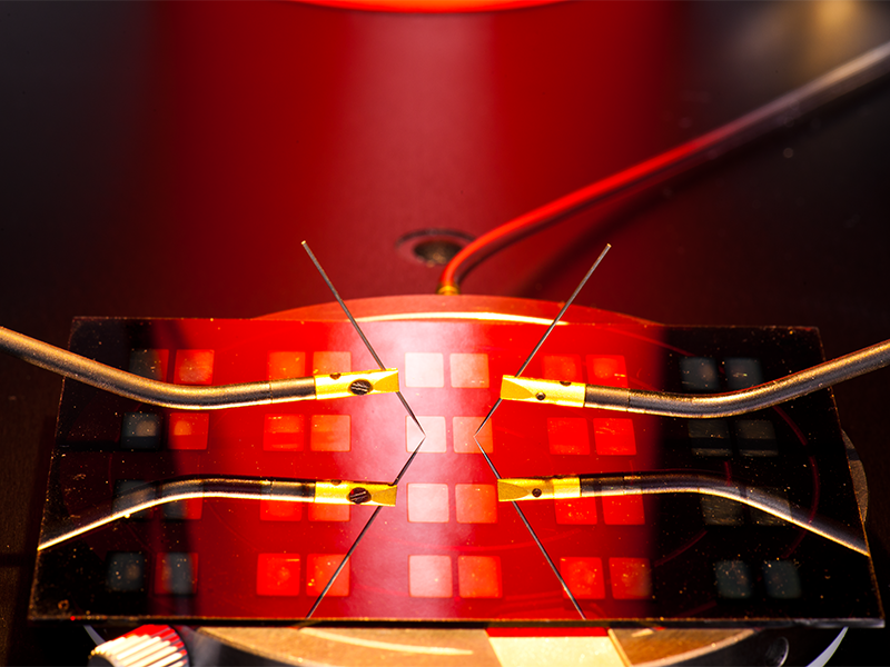
Determination of electrical conductivity (SÜSS Prober and Keithley)
Corrosion and climate tests
- Corrosion test system for condensation water test and salt spray test, SKB 400 A-SC (Liebisch)
- Environmental chamber -40 ... 150°C with adjustable humidity, SH-241 (ESPEC)