Ion beam preparation of cross sections for high resolution FE-SEM investigations of thin film solar cells

The efficiency of thin film solar cells is substantially affected by structure and interfaces between absorber layer, front contact and back contact. High resolution FE-SEM investigations are able to make an important contribution for the further optimization..
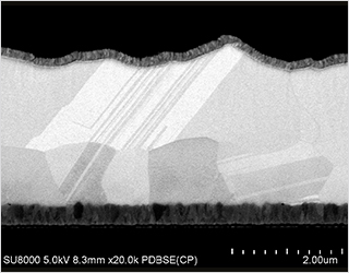
Ion polished cross sections can be prepared through the whole layer stack of thin film solar cells by means of broad ion beam (BIB) technique available at Fraunhofer FEP. Thereby it is possible to investigate structure and interfaces between absorber layer and different thin films of front and back contact of the solar cell by high resolution field emission scanning electron microscopy (FE-SEM).
The imaging of ion polished cross sections is carried out with backscattered electrons in material and crystal orientation contrast. The microstructure of polycrystalline absorber layer can be characterized in respect of present lattice defects as grain boundaries, dislocations and twins. Simultaneously the interfaces between absorber layer, front and back contact layers can be investigated at high resolution.
The present interfaces are potential recombination centers for charge carriers and have to be optimally adapted in respect of structure and doping.
An enhancement of the absorption of the solar radiation in short and long wavelength range is achieved by chemical gradients within the absorber layer which can be analyzed by energy dispersive spectrometry of x-rays (EDS). By optimization of this chemical gradients the band gap of the absorber material can be adjusted that high quantum efficiencies can be achieved for a broad spectral range.
The influence of microstructure of polycrystalline thin film solar cells on the separation and diffusion of photo generated charge carriers can be evaluated by FE-SEM imaging and simultaneous registration of the signal distribution of electron beam induced current (EBIC). This enables for example a direct investigation of the effect of grain boundaries on the local EBIC signal distribution.
Additionally, the analysis of the EBIC signal distribution enables the evaluation of the position of the pn junction and of the mean diffusion length of the charge carriers.
The comprehensive analytical opportunities provide an important contribution for further enhancement of the efficiency of thin film solar cells.
 Fraunhofer Institute for Electron Beam