 Fraunhofer Institute for Electron Beam
Electron beam machine for surface structuring and for fine and micro welding processes

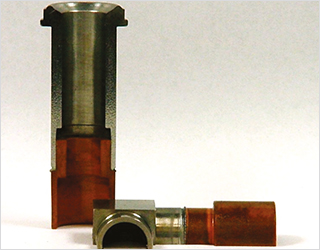
An electron beam is a versatile tool whose effect is primarily based on a short-duration, localized input of heat into a substrate material. An important advantage of electron beam welding is the ability to be able to weld materials down to considerable depths: although strongly absorbed by the material, the electron beam is able to penetrate deep into the material due to the deep-weld effect. This makes this technique an ideal tool for joining combinations of materials.
Of all welding techniques, electron beam welding currently involves the lowest heat input for a given weld depth. Due to this minimum heat input, thermally sensitive sensors can, for example, be welded.
The electron beam can also be used to structure surfaces. Due to the minimum heat input on the workpiece, an electron beam is ideal for processing thermally sensitive materials such as metal layers on polymer substrates. Reactive materials can also be effectively processed because the process takes place in a high vacuum and the reactive metals are not in contact with reaction partners.
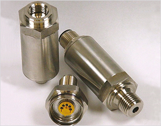
Our electron beam plant EFFI can be used to weld, structure and engrave small parts made of conducting materials having a height and diameter of up to 15 centimeters.
Typical tasks that can be carried out in the machine include the welding of medical products (such as implants) and the welding of sensors and devices used in electronics and measuring technology.
| Electron beam generator | Beam power up to 2 kW / acceleration voltage up to 60 kV Max. beam deviation angle α ≤ ± 20° |
| Workpiece insertion and handling | 1 axis of rotation (Z), chuck with clamping diameter of 3 ... 88 mm Rotation speed: continuous from 0 ... 32 min-1 Vertical translation (Y): 120 mm Vertical adjustment speed: 0 ... 3.5 mm/s Substrate (part) size up to 150 mm × 150 mm × 150 mm (L × W × H) |
| Vacuum system | Working pressure (chamber) ≤ 5 × 10⁻⁴ mbar Short cycle times, as evacuation time < 2 min and pressurization time < 30 s |
| SEM imaging system | Scanning electron imaging mode (SEM) with a choice of two detectors Display in material and/or topographic contrast, max. scanned area ca. 100 × 150 mm2 Resolution down to 25 μm |
| Process control | Teach-in programming Automatic standard welding processes / programmed deflection control Alternating operating mode welding-scanning-welding Engraving of any grayscale images |