Sputter epitaxy

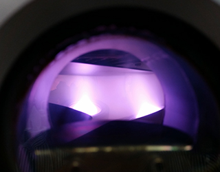
Magnetron sputter epitaxy (MSE, or sputter epitaxy for short) is a pioneering technology for the deposition of III-nitride semiconductors such as aluminum nitride (AlN) and gallium nitride (GaN). III-nitride semiconductors serve as the basis for future high-performance electronic components in applications such as power electronics, high-frequency technology and optoelectronics.

The unique properties of AlN and GaN are high electron mobilities, high thermal conductivities, good thermal and chemical stabilities, very large band gaps and high electric field strengths. These properties are crucial for the efficiency and performance of power electronic devices such as HEMTs (High-Electron-Mobility Transistors), vertical transistors, diodes and LEDs, as they enable improved heat dissipation, higher dielectric strength, faster switching speeds, and higher quantum yields.

What is sputter epitaxy?

Sputter epitaxy is a physical vapour deposition (PVD) process in which atoms are removed from a target surface and deposited on a substrate in a controlled manner. This technique enables the precise production of epitaxial (crystalline), semiconducting thin films with specific electrical and optical properties that are suitable for a wide range of applications.

Sputter epitaxy enables precise control over film properties and allows the production of high quality, high performance electronic devices critical to the growing demands of power electronics and wireless communications.

Advances in sputter epitaxy

Current research at Fraunhofer FEP focuses on the control of morphology, crystal quality (epitaxy) and polarity in III-nitride layers, in particular through the use of aluminum nucleation layers. Key findings include:

  • Improvement of crystal quality: X-ray diffraction measurements show that the use of Al nucleation layers significantly improves the crystal quality of AlN and GaN layers.
  • Morphology and polarity: Nanoscale structural and chemical investigations using scanning transmission electron microscopy (STEM) show that Al nucleation influences the polarity of the AlN layers. This enables the targeted production of both metal-polar and N-polar layers on a macroscopic scale.
  • Technological relevance: The control of layer polarity is an important technological milestone for the development of even more efficient next-generation electronic devices.

Research and development at the Fraunhofer FEP

In future, innovative processes are to be developed at the Fraunhofer FEP to further increase the efficiency and quality of sputtering processes and heteroepitaxial layers and to adapt them to the needs of industry. In particular, nitride epitaxy is to be made possible on wafer diameters of up to 200 mm.

Sputter epitaxy enables a more resource-efficient and energy-efficient production of nitride semiconductors compared to conventional methods such as MOCVD (metal organic chemical vapour deposition) and makes a decisive contribution to the further development of III-nitride technology. Sputter epitaxy opens up new perspectives for the application of nitride semiconductors in power electronics, especially for power converters, power amplifiers and optoelectronic components.

Weitere Informationen


International Workshop on Magnetron Sputter Epitaxy

Die internationale Magnetronsputter-Epitaxie-Plattform zum Austausch und zur Vernetzung in Wissenschaft und Industrie.