Single substrate coating

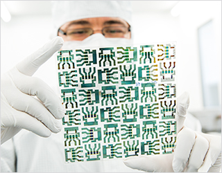
We offer specialized coating processes for single substrates such as wafers and glass substrates that are specifically tailored to the requirements of modern microelectronics, optics and sensor technology.

Our technologies, including reactive pulse magnetron sputtering, magnetron PECVD and electron beam evaporation, enable the development of coatings with optical, electrical, acoustic, magnetic or corrosion-inhibiting properties.

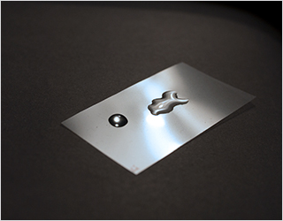
Through the targeted control of substrate movement and precise in-situ monitoring, we can realize coating thicknesses and properties with high reproducibility and long-term stability. These processes ensure high efficiency and flexibility, making them ideal for customized solutions and complex coating requirements.

Whether for glass, wafers or other materials, our coatings set standards in quality and precision and offer a wide range of applications for various high-tech industries.

Our offer

Fraunhofer FEP offers comprehensive expertise in process and technology development for coating technologies and layer systems according to your application along the entire value chain:

  • Feasibility studies
  • Development of the coating technology and coating system for your product
  • Sample coatings
  • Development of key assemblies
  • Technology transfer to production
  • Support with system realization for our customers
  • Licensing

This development work is supplemented and supported by

  • Acquisition and coordination of projects subsidized by the state, the federal government and the European Union
  • Economic feasibility studies
  • Studies on the state of the art, e.g. literature and patent research

Technologies

Electron beam evaporation

also in combination with plasma processes.

Stationary coating

In stationary sputtering, the substrate remains in front of the sputter source. It is used for single substrate coating (300 mm to 450 mm in future) or several small substrates on a carrier in cluster systems.

Reactive pulse magnetron sputtering and magnetron PECVD

Efficient methods for producing specific compound layers with high coating rates and precise layers.

Electron beam deposition

also in combination with plasma processes

Applications

Optical interference layer systems

  • Optical filters for laser optics, spectroscopy applications
  • Anti-reflective coatings

Piezoelectric coatings

  • for microsystems (MEMS), BAW, SAW
  • for ultrasound microscopy
  • for micro-energy harvesting systems
  • for micro-energy harvesting (energy harvesting)
  • for force sensors
  • for electro-optical transducers

Electrical insulation layers

  • for sensors (e.g. component-integrated)
  • for microelectronics
  • for photovoltaics
  • for assembly and connection technology
  • also on structured or rough substrates

Wetting-promoting coatings, superhydrophilic coatings

  • for sensor technology
  • for electrocalorics

Direct metallization of plastics

  • for EMC shielding

Permeation barrier layers and functional layers

  • for hydrogen applications
  • for electrolysis and fuel cells
  • Etch stop, moisture barriers and protective coatings
  • High-k dielectrics

ta-C coatings

Ceramic thin films

Biocompatible coatings

  • for metallic tools
  • for implants

Anti-corrosion coating


Our facilities


Cluster 300

Test facility for stationary magnetron sputtering of flat substrates with a diameter of up to 300 mm

Cluster 250

Cluster system


ERICA

Cluster system for complex coating and structuring processes in vacuum


MAXI

In-line coating system for sheets and metallic strips

BesTec

Universal test system for PVD processes, low-temperature processes and inert handling


UNIVERSA

Batch system for coating 3D substrates


NOVELLA

Test facility for coating components

Combination processes of plasma-activated high-rate evaporation, magnetron sputtering and PECVD

Sputterepitaxy system

Magna

preciTurn