 Fraunhofer Institute for Electron Beam
ILA 750

Special sun-protective glasses
Functional layers and layer stacks are applied to flat substrates at the Fraunhofer FEP using magnetron sputtering. Our core expertise in this field is pulse magnetron sputtering (PMS). The first step is to identify suitable layers and layer stacks that give the desired properties for specific applications. By developing and adapting the sputtering process for the respective task we optimize the deposition process in order to get high quality layers to be realized at favorable cost.
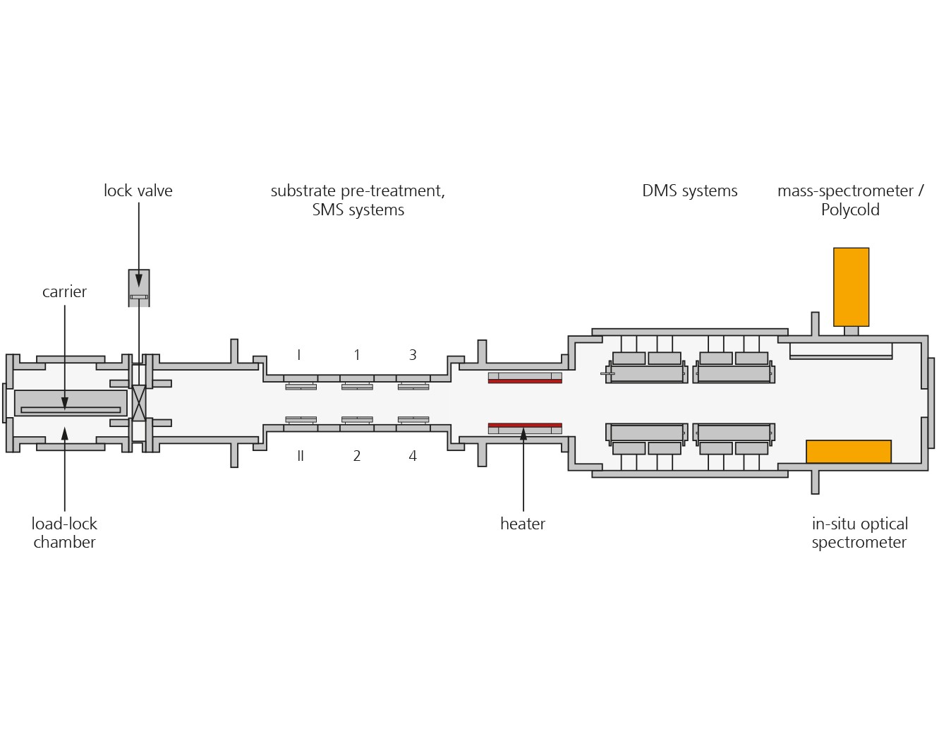
The ILA 750 is our in-line sputtering plant which we use to develop layers, layer stacks, and sputtering processes in a highly efficient way. Flat substrates made of glass, polycarbonate, other polymers, metal sheets, and ceramics can be coated with various layers (metal, metal oxide, metal nitride, and metal oxynitride layers) using reactive and non-reactive sputtering processes. If further scale-up of the process is required, the in-line sputtering plant ILA 900 gives us the option to apply layers and layer stacks on substrates having maximum dimensions of 1200 × 600 × 60 millimeters. Besides the development of layers, layer stacks, and processes, the Fraunhofer FEP has expertise in developing prototypes of key components for pulse magnetron sputtering.
Example applications of the layers and layer stacks are architectural glass (low-E coatings /solar control coatings), transparent conducting electrodes (TCO / IMI layer stacks), and electromagnetic shielding (EMI) and antireflection coatings and antireflection-antistatic coatings in displays in electronic and photovoltaic devices.
Technologies
- In-line substrate pre-treatment
- Magnetron sputtering (DC, HF, MF, pulse DC)
- dynamic deposition
- vertical deposition for low particle generation
- inlet of special gases (e. g. H2)
Technical specifications
| Chambers | 1 process chamber, 1 load-lock chamber |
| Coating sources on each side of the plant | 2 dual magnetron sputter systems 2 single magnetron sputter systems |
| Substrate pre-treatment | etching and heating (up to 350°C) |
| In-situ optical reflection and transmission measurement | |
| Reactive processes | metal oxides / nitrides / oxynitrides |
| Non-reactive processes | metals and conducting oxides, magnetic metallic layers |
| Deposition width (material-dependent) | 500 mm (+/- 2% layer thickness homogeneity), 600 mm (+/- 5% layer thickness homogeneity) |
| Max. substrate dimensions | 400 mm × 600 mm |
| Substrate thickness | up to 60 mm |
| Carrier speed | 0.01 ... 3 m/min |
| Base pressure | 3 × 10⁻⁶ mbar |
| Working pressure | 10-4 ... 10-2 mbar |
| Loading under clean room conditions | |
| Programmable sequence control |
Our offer
- Feasibility studies
- Development of sputtering processes and functional layer stacks and single layers under near-real production conditions
- Small series production
- Supply of key components
- Technology transfer