 Fraunhofer Institute for Electron Beam
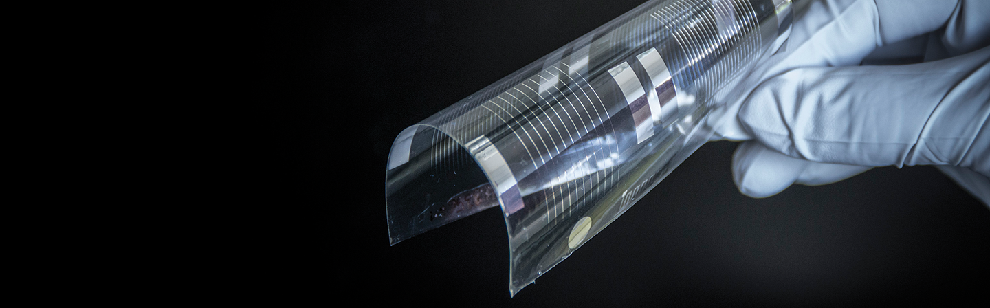
21 | 2017 – Biodegradable electronics
Under the direction of the Fraunhofer Institute for Organic Electronics, Electron Beam and Plasma Technology FEP, an in-house Fraunhofer project for development of biodegradable electronics was begun last year. The Fraunhofer Institute for Electronic Nano Systems ENAS, the Fraunhofer Institute for Biomedical Engineering IBMT, the Fraunhofer Institute for Silicate Research ISC, and the Fraunhofer Resource Recycling and Strategy Project Group IWKS are working together on the project. The first results of the Fraunhofer FEP will be presented during Semicon Europe 2017 as part of productronica 2017 in Munich at the Silicon-Saxony joint booth in Hall B, Booth Nr. B1-416, November 14-17, 2017.
Electronic components that are completely broken down in a biological environment after a pre-defined operating life open up novel applications as well as ways for reducing their ecological footprint.
One enabling technology for such components is the manufacture of biodegradable conductive traces on biodegradable substrates using vacuum technologies. This technology was developed by Fraunhofer FEP.
A novel application area for these innovative electronic components for example is in the field of active medical implants that after expiration of their operating life are resorbed by tissue, thereby sparing the patient a second surgical intervention.
The Fraunhofer Gesellschaft e. V. is now funding the “bioElektron – Biodegradable Electronics for Active Implants" project through its in-house program (funding No. MAVO B31 301). The goal of the project is the development of essential components for biodegradable electronic parts that can be employed for example in an implant.
This includes in particular
- biodegradable conductor structures
- biodegradable electrodes for collecting electrical signals or delivering electrical stimulation
- biodegradable thin-film transistors and circuitry
- biodegradable barrier coatings as moisture and gas barriers, and electrical insulation layers
These elements will be monolithically integrated into a flexible thin-film device.
Conductor structures and organic thin-film transistors are being developed at Fraunhofer FEP using vacuum technology. Deposition of magnesium via thermal evaporation under high vacuum conditions is being used as an enabling technology for this purpose. Magnesium is known for being a biodegradable and biologically compatible metal that is already employed in clinical environments as an absorbable implant material. The challenge consists of depositing this metal upon biodegradable polymer films that magnesium does not adhere sufficiently to under normal process control. By suitably pre-treating the substrates using a combination of drying, plasma treatment, and utilization of seed layers, finely structured high-quality conductor structures were able to be produced.
“We are now prepared to discuss these results with interested partners from industry and the scientific community during productronica 2017 at the Silicon-Saxony joint booth (Hall B1, Booth B1-416) in order to be able to implement them in current practical applications”, explains Dr. Michael Hoffmann from Fraunhofer FEP and head of the bioElektron project.
About bioELEKTRON:
www.fep.fraunhofer.de/en/ueber-uns/projekte/bioElektron.html
2017FLEX Europe Conference
Trade-fair booth: Silicon-Saxony joint booth in Hall B1, Booth No. B1-416
Talks:
Wednesday, 15.11.2017, 2:35 pm, ICM 1st floor, Room 14c
„Biodegradable flexible conductor structures“, Dr. Michael Hoffmann, Fraunhofer FEP
Wednesday, 15.11.2017, 10:45 am, Hall B1 TechLounge / B1.168
CMOS based microdisplays, imagers, sensors by OLED/OPD, Bernd Richter, Fraunhofer FEP
Innovation Forum
Hall B2, next to booth no. 457 OE-A Organic and Printed Electronics Association
Wednesday, 15.11.2017, 3:00 pm, Hall B2 / 453
Session: Printed Electronics Insights: Advancing Wearables
Electronics and OLED lighting in textiles, Jan Hesse, Fraunhofer FEP
Thursday, 16.11.2017, 3:00 pm, Halle B2 / 453
Session: Printed Electronics Insights: Applications and New Developments
Ultra-thin glass as a substrate and encapsulant for bendable OLED devices fabricated in Roll-to-Roll, Dr. Stefan Mogck, Fraunhofer FEP
Last modified: