 Fraunhofer Institute for Electron Beam
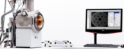
01 | 2014 – Precise microprocessing with electron beam
Fraunhofer FEP and FOCUS electronics GmbH launched activities to make the advantages of electron beam machining industrially available for large-scale microprocessing tasks and surface layer treatments.
Microprocessing, in other words, the precise cutting, removal, joining and modification of structure on a micrometer scale, is widely used in fields such as photovoltaics, medical technology or mechanical engineering. For example, stents for medical technology are cut to micrometer accuracy, sensitive sensors are welded and wafer-based solar cells are structured and equipped with electrical contacts. The laser is a common tool for these machining processes. The »electron beam« is a much lesser known and used tool for this work. However, considering its special physical properties, the electron beam is ideal for microprocessing and opens up new possibilities for application. Compared to a laser, it has great potential especially for structuring of optically transparent layers as well as deep-set or thicker layers.
The electron beam has long been established as a tool in industrial manufacturing for welding, melting and evaporating metals or for material analysis. In the »EMICPRO« project FOCUS electronics GmbH and the Fraunhofer Institute for Electron Beam and Plasma Technology FEP are now carrying out basic tests to make use of potential of electron beams for micro processing in micro systems technology a s well as surface and thin-film technology.
Surfaces can be treated with the electron beam with diameter of 1 … 100 μm in a much cost-efficient and productive way. One big advantage of the electron beam is that various processes such as structuring, electrical contacting or similar are possible with a single, highly-productive beam source by simply changing the operating parameters. This greatly simplifies handling during the process and saves costs since only one beam source is needed. Another advantage is that electron beams penetrate deeper into the workpiece, thus allowing a precise treatment of deeper or thicker layers. This means that high-energy electrons can penetrate several tens of micrometers into a solid body with energies of around 50 keV. The thermal effect on the base material can be minimized through selective energy input into the volume of the layer to be treated.
The process does not require mechanical deflection systems, optical lenses or mirrors that are susceptible to soiling. The almost inertia-free electro-magnetic deflectability of the electron beam allows a high writing speed and hence the desired productivity as well as a good process reproducibility. The aim of the »EMICPRO« project is to integrate an electron beam microprocessing station in a vacuum-in-line coating system and to investigate new beam source concepts and the ways to control them. The project also aims to develop an electron beam source for microprocessing. This source should have a high beam brilliance (i.e. low image distortion) and at the same time a high power density, large deflection angle (± 35°) and a high deflection frequency (100 kHz large signal). In addition, the source should have a long service life and long-term stability, particularly in fine vacuum processes.

Download the press release and picture
Last modified: