 Fraunhofer Institute for Electron Beam
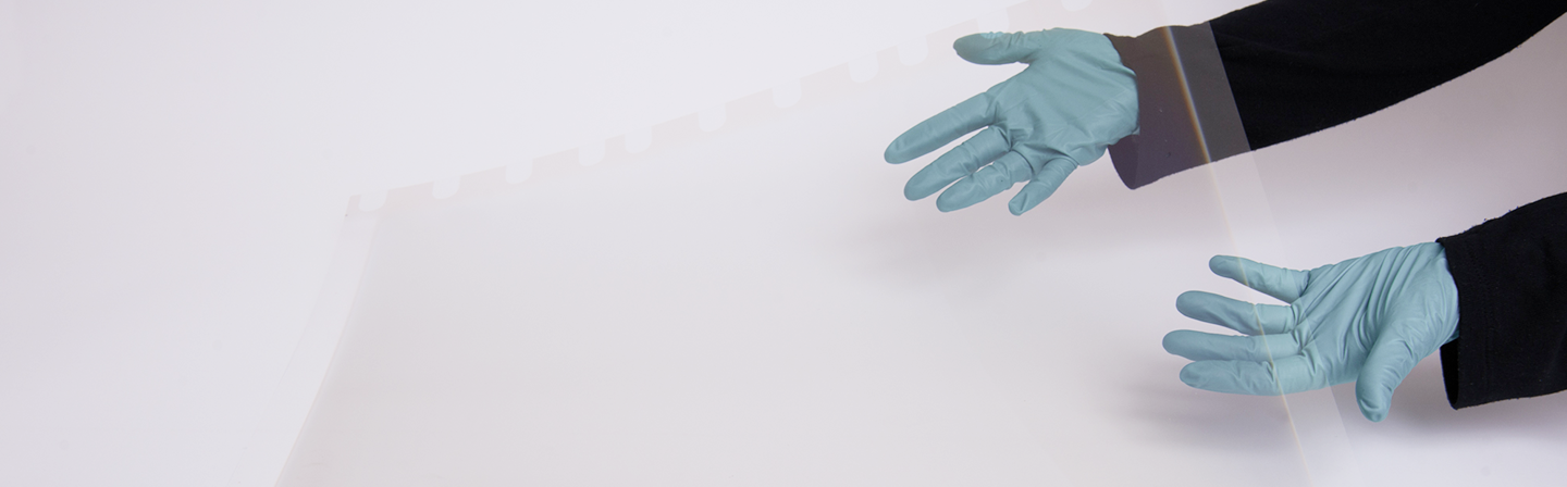
02 | 2020 – Flash lamp annealing: Energy-effective process for efficient annealing of large-area substrates
In thin-film technology, heat treatment – also referred to as annealing – is often used to selectively improve material properties of thin films, such as their crystallinity or density, and hence their electrical and optical properties. However, these are energy-intensive as well as time-intensive techniques, associated with large facility footprints. That makes their applicability for large-area substrate formats difficult or even impossible. Flash lamp annealing (FLA) offers a smart solution to this problem. In cooperation between ROVAK GmbH and the Fraunhofer Institute for Organic Electronics, Electron Beam and Plasma Technology FEP this technology has been studied and further developed for large-area applications as part of the project InnoFlash funded by the Saxony State Ministry of Economy, Labor and Transport (SMWA, project number 100349243/3698).
Thermal treatment of coated glass, plastics and wafers is a common process for improving the layer and surface properties of large-area substrates. In conventional furnace-annealing processes, the entire substrate is heated and must cool down slowly after the treatment. This is time and energy intensive and can be problematic for treating large substrate areas. In addition, long thermal processes for thin-film technology lead to undesirable diffusion phenomena and may therefore require additional diffusion suppressing barrier layers. The production process thus becomes more complex. FLA offers a good alternative to conventional furnace annealing for the optimization of film properties, e. g. electrical and optical properties, especially on large-area substrates.
FLA is an innovative process for thermal pre- and post-treatment of functional coatings and sensitive substrates using xenon flash lamps working in a time period of only a few milliseconds. A significant advantage compared to conventional processes is the application of thermal energy to a restricted a local area on the substrate (such as just the surface, for example). This reduces the thermal load and hence the temperature throughout the entire substrate. Thus, this process is more efficient and less expensive compared to furnace processes. Due to the small footprint of the FLA setup, this process can be implemented into almost any production line. Moreover, FLA is less energy-intensive, which results in a reduction of CO2 emissions.
In collaboration with ROVAK GmbH, researchers of the Fraunhofer FEP are investigating and experimenting with new electrical circuit designs for energizing flash lamps as well as for enhancing process control and measurement technology. ROVAK's know-how in the field of technology and system development for pulsed high-power flash lamps provides the foundation for this advanced work.
Dr. Manuela Junghähnel, head of the Sheet-to-Sheet Technologies and Precision Coating department at Fraunhofer FEP, explains: “We have focused on inline FLA. Our investigations have enabled us to treat large surface areas under conditions of continuous operation. Treatment speeds of up to 6 meters per minute and widths of up to 3.2 meters are feasible. This annealing method primarily treats just the regions close to the surface. It also allows the processing of temperature-sensitive materials, whereat a maximum surface temperature of up to 2,000°C can be achieved.”
Operation of long flash lamps (up to 1000 mm) was investigated for treating large substrate areas. The difficulty was to ensure a safe and reproducible flash operation, since a reliable flash ignition as well as a uniform distribution of the deposited energy density are necessary characteristics for high-quality treatment. In addition, handling the high currents and voltages that occur in the millisecond range for the FLA process posed a challenge. Effective process control is necessary for using FLA in industrial applications. To accomplish this, a measuring system has been investigated to record the temperature profile of the surface during treatment using time-resolved emission detection. This allows the exact determination of the annealing effect of each individual flash.
FLA in its conventional form has already reached the marketability stage. After completion of the investigations at the Fraunhofer FEP, the results of the project will be able to be used by ROVAK to launch FLA systems adapted for efficient, large-area treatment.
Project partner
ROVAK GmbH
Grumbach
www.rovak-flash-lamp.com
Fraunhofer FEP auf der ICCG13
March 23– 26, 2020 in Braunschweig
https://13.iccg.eu
Booth No.: C1
Techtalks:
March 24, 2020, Session 3
Film growth metrology, process control, simulation
Recent developments in dynamic flash lamp annealing for ultra-fast thermal annealing of large substrate areas
Thomas Preußner, Fraunhofer FEP
16:10 PM - 16:30 PM
March 24 – 25 2020, Session 4
Energy conversion, lighting, displays
Chairpersons: Dr. Manuela Junghähnel (Fraunhofer FEP), Dr. D. Bernt
Poster:
March 26, 2020
Posters will be on display throughout the conference. Poster presentations by the authors will take place on Tuesday afternoon, March 26.
Last modified: