 Fraunhofer Institute for Electron Beam
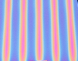
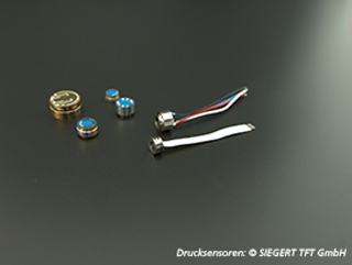
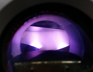
The Fraunhofer FEP offers advanced technological solutions for the growth sectors of optics, sensor technology and electronics. Our coating technologies are becoming increasingly important as they both optimize existing products and enable new product innovations. With our many years of experience and state-of-the-art system technology, we are able to apply electrical, optical, acoustic and magnetic coatings precisely and homogeneously to large surfaces.
Our vacuum processes ensure high coating rates, accuracy and reliability, which guarantees the productive and cost-effective manufacture of sophisticated products. The use of electron beam technology also enables us to weld sensitive material combinations with extreme precision, particularly in the field of sensor technology, and to create solutions that would not be possible with other processes.