 Fraunhofer Institute for Electron Beam
Investment in a new atomic force microscope
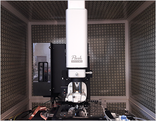
The investment in a new NX20 atomic force microscope from Park Systems GmbH has considerably improved the characterization capabilities for thin films at Fraunhofer FEP.
The device features a motorized XY table with a working area of 150 mm × 150 mm (6” × 6”). The measurements can thus be automated to a great extent and carried out with very high efficiency.
In non-contact mode, roughness of thin films can be determined with high horizontal and vertical resolution. Low roughness is desired for many optical coating systems in order to achieve the lowest possible scattering of light, for example. Another important application is topographical imaging for epitaxial layers. Here, AFM imaging can be used to investigate the type of layer growth and the quality of crystal with respect to lattice defects, both of which are crucial for utilizing these layers.
In addition, the instrument has other modes for determining physical properties such as electrical conductivity, piezoelectric deflection, and modulus of elasticity, which open up new, interesting application opportunities.