 Fraunhofer Institute for Electron Beam
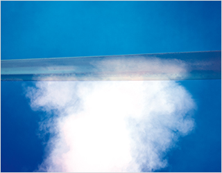
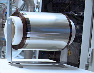
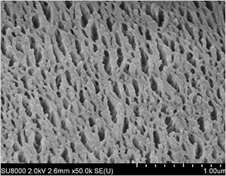
Plasma-assisted coating processes enable the production of customized coatings for many areas of application. Our strength lies in qualifying these plasma-assisted coating processes for industrial production and the coating of large surfaces. The core competence includes the PVD processes of plasma-activated high-rate evaporation and pulse magnetron sputtering as well as PECVD processes for plasma-activated chemical vapour deposition with various high-performance plasma sources.
A unique selling point is the combination of extremely dense plasmas with extremely high deposition rates for the economical deposition of high-quality coatings. The combination of economic efficiency with precision in terms of process control and coating properties opens up new applications. For these coating processes, we also develop the cleaning processes and plasma pre-treatments required to ensure coating adhesion.